
Hacking the T2S+ Out of Fear: Get Lock-In Thermography for Free link
September 29, 2024
Updated: July 16, 2025
By now you have probably seen the sea of cheap Chinese thermal cameras meant to plug into your phone that have flooded the market, and quite quickly out-competed stuff like the FLIR smartphone plugins. The reasons are pretty simple: they have higher refresh rates and often better resolutions. Recently, I became the owner of one of these cameras.
Now before I begin telling the story and try to explain everything, I should preface this with the disclaimer that the following information is what I was able to piece together from internet rumors and plausible guesses. There is not that much information on these out there, so if you know something and wish to correct me, please reach out. My email is in the footer of every page on this site.
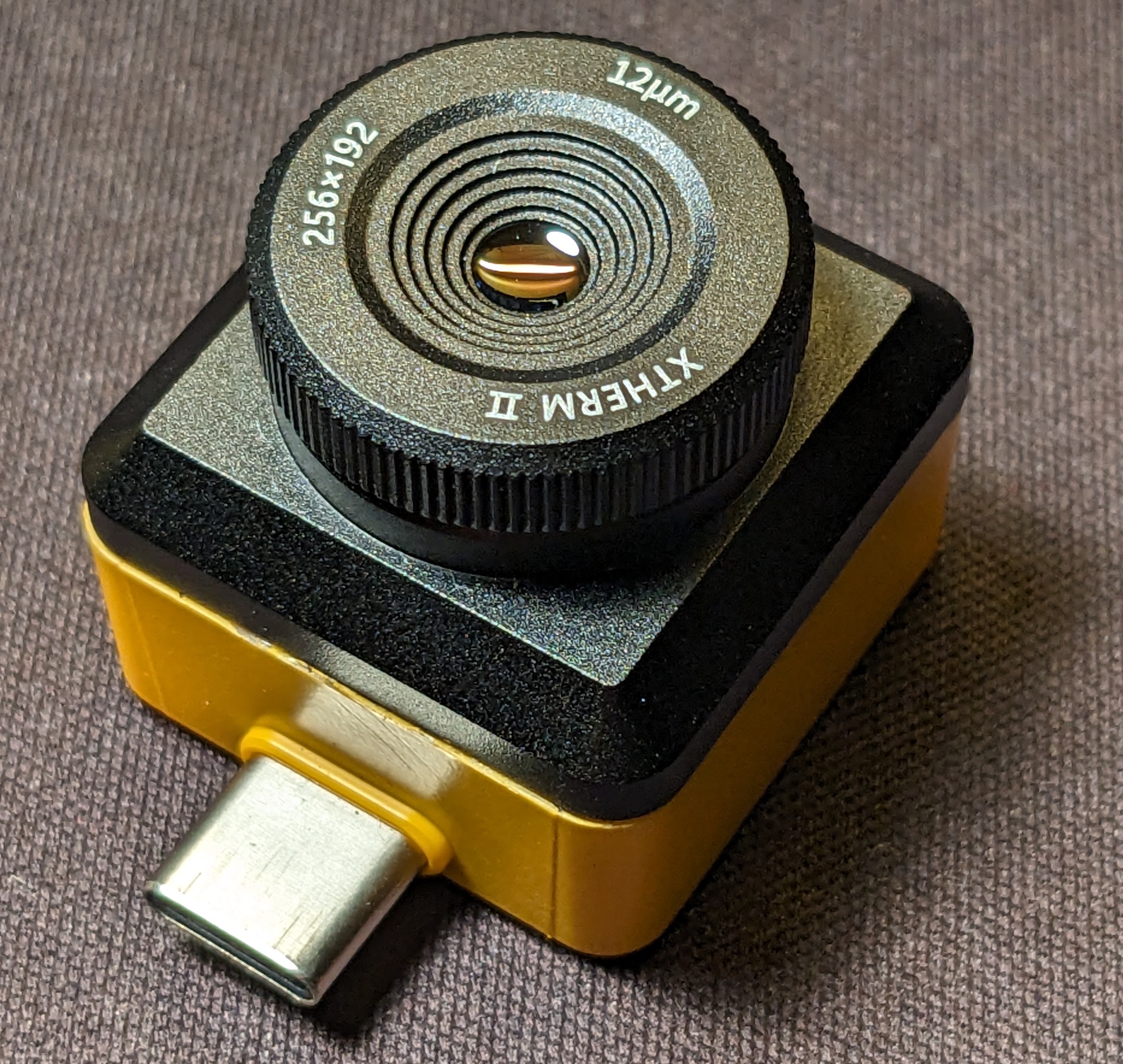
The camera unit I got is branded as an "Xinfrared Xtherm II T2S+", originally purchased in late 2023. When you use the official app (mirror) (on an air-gapped burner phone, we'll get to why that's a good idea later), it works okay, but the app is sometimes buggy, crashes when changing settings, and phones home for some reason.
So, without much thought I connected it to a computer, ran lsusb and it showed up
as:
Bus 001 Device 019: ID 04b4:0100 Cypress Semiconductor Corp. Cino FuzzyScan F760-B
And it showed up as a webcam according to v4l2-ctl --list-devices:
T2S+ (usb-0000:00:14.0-1):
        /dev/video14
        /dev/video15
        /dev/media2
So, I tried capturing an image with fswebcam -r 256x196 --png 0 --no-underlay --no-banner -D 1 p.png
and got this...

At this point, I realized that I got the "V2" of the camera. This camera is regarded as worse than the "V1" mostly because the manufacturer removed the internal processing FPGA? (That's what people say on the forums, but that doesn't seem to be the case, teardown later in this post). And now we are basically getting raw temperature readings from the sensor.
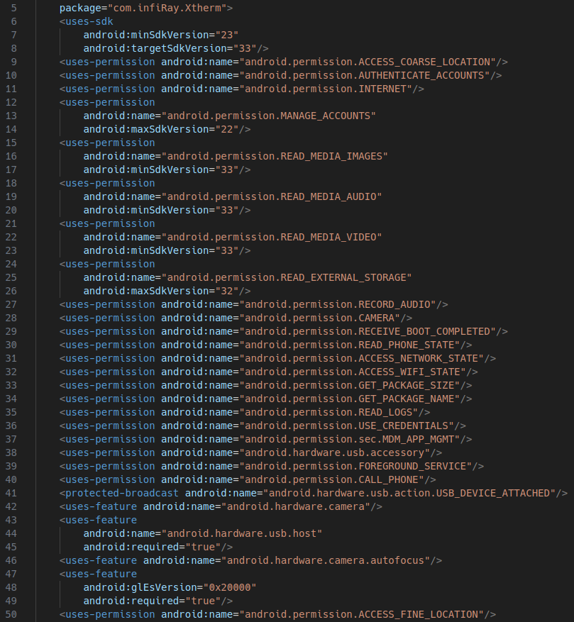
I started by decompiling the Xtherm Android app using jadx-1.5.0. To my surprise, it wasn't even obfuscated; almost everything was just readable code with variable, class names, and everything. However, this revealed that first of all, the code is super cursed and looks like a bunch of random examples thrown together a bit dirtily (explains the random crashes). The app also has a bunch of analytics and a worrying amount of permission requests for something that should just display the image from a USB camera. Here is a non exhaustive list of the most interesting ones:
- ACCESS_COARSE_LOCATION - Allows an app to access approximate location.
- ACCESS_FINE_LOCATION - Allows an app to access precise location.
- AUTHENTICATE_ACCOUNTS - Allows an app to act as an AccountAuthenticator for the AccountManager.
- MANAGE_ACCOUNTS - Allows an app to manage the list of accounts in the AccountManager.
- USE_CREDENTIALS - Allows an app to request authtokens from the AccountManager.
- READ_PHONE_STATE - Allows read access to phone state, including the current cellular network information, phone number, the status of any ongoing calls, and a list of any PhoneAccounts registered on the device.
- RECEIVE_BOOT_COMPLETED - Allows an app to receive the ACTION_BOOT_COMPLETED that is broadcast after the system finishes booting. This allows the app to start automatically when the device boots up.
- CALL_PHONE - Allows an app to initiate a phone call without going through the Dialer user interface for the user to confirm the call.
- READ_LOGS - Allows an application to read the low-level system log files. Log entries can contain the user's private information.
- SYSTEM_ALERT_WINDOW - Allows an app to create windows using TYPE_APPLICATION_OVERLAY, shown on top of all other apps. Very few apps should use this permission; these windows are intended for system-level interaction with the user.
- MOUNT_UNMOUNT_FILESYSTEMS - Allows mounting and unmounting file systems for removable storage. Not for use by third-party applications.
- WRITE_SETTINGS - Allows an application to read or write the system settings.
- GET_TASKS - Allows an application to get information about the currently or recently running tasks.
- ACCESS_WIFI_STATE - Allows applications to access information about Wi-Fi networks.
- CHANGE_WIFI_STATE - Allows applications to change Wi-Fi connectivity state.
- RECEIVE_USER_PRESENT - Allow an app to receive a broadcast when the screen is on or has been unlocked.
- WAKE_LOCK - Allows using PowerManager WakeLocks to keep processor from sleeping or screen from dimming.
- ACCESS_LOCATION_EXTRA_COMMANDS - Allows an application to access extra location provider commands.
- ACCESS_NETWORK_STATE - Allows applications to access information about networks.
- CHANGE_NETWORK_STATE - Allows applications to change network connectivity state.
- WRITE_EXTERNAL_STORAGE - Allows an application to write to external storage.
- MDM_APP_MGMT - Allows an application to perform MDM (Mobile Device Management) tasks related to application management. (Note: This permission is typically used by system apps or device policy management apps.)
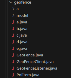
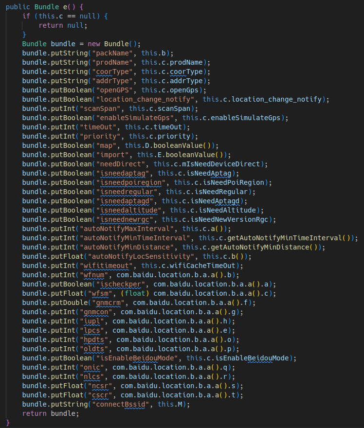
Here are some curious snippets from the decomp: (Click to enlarge)

000yesnt has also decompiled the app and analyzed what the permissions are actually used for. For more info please visit their writeup.
The decompilation also revealed the fact that most of the processing actually happens in elusive shared objects that
aren't as easy to decompile compared to the rest of the Java app. I started with the file named
libthermometry.so.
This is because while capturing a log of the app running, I got it to enter some sort of error that revealed a bunch
of useful debug info, and it was all linked to this file.
libUVCCamera: [20119*serenegiant_usb_UVCCamera.cpp:226:nativeGetByteArrayTemperaturePara]:nativeGetByteArrayTemperaturePara:0,0,0,0,0
jsonObject: {"doAction":1,"deviceSn":"ME1299","deviceModel":"google,Pixel 3","deviceNo":"T2S+","appVersion":"6.7.240509","osVersion":"Android12,level31"}
libUVCCamera: [20206*thermometry.c:367:EAthermometryT4Line]:EAthermometryT4Line start
libUVCCamera: [20206*thermometry.c:368:EAthermometryT4Line]:correction:0.000000, Refltmp:25.000000,Airtmp:25.000000 ,humi:0.450000,emiss:0.980000,distance:1
libUVCCamera: [20206*thermometry.c:417:EAthermometryT4Line]:shutTemper:451
libUVCCamera: [20206*thermometry.c:446:EAthermometryT4Line]:a:0.234700, b:31.179001, ka:-0.000010, kb:0.008200, kc:0.745000
libUVCCamera: [20206*thermometry.c:458:EAthermometryT4Line]:correction:0.000000, Refltmp:25.000000, Airtmp:25.000000, humi:0.450000, emiss:0.980000, distance:1
libUVCCamera: [20206*thermometry.c:486:EAthermometryT4Line]:WriteTable  fpatemp:29.53, shuttemp:27.59, floatShutTemper:28.19, shutterFix:-0.60
libUVCCamera: [20206*thermometry.c:549:EAthermometryT4Line]:EAthermometryT4Line end
MediaPlayerNative: pause called in state 8, mPlayer(0x78c52c1eb0)
MediaPlayerNative: error (-38, 0)
MainActivity: rangeMax:43.7
MainActivity: rangeMin:29.6
MainActivity: v:29.6,v1:43.7
tnn     : void UVCCamera::setTempDiv(float, float, int, int, int) [File jni/UVCCamera/UVCCamera.cpp][Line 663] begin
tnn     : virtual void UVCPreviewIR::setTempDiv(float, float, int, int, int) [File jni/UVCCamera/UVCPreviewIR.cpp][Line 2640] begin
tnn     : virtual void UVCPreviewIR::setTempDiv(float, float, int, int, int) [File jni/UVCCamera/UVCPreviewIR.cpp][Line 2642] end
tnn     : void UVCCamera::setTempDiv(float, float, int, int, int) [File jni/UVCCamera/UVCCamera.cpp][Line 668] end
MediaPlayerNative: invoke failed: wrong state 0, mPlayer(0x78c52c1eb0)
So that's where I started. I threw the binary into Ghidra. (For those who don't know, Ghidra is an open-source reverse engineering tool for this exact thing, developed by... the NSA...).
I was also able to just directly download this file from the Xinfrared SDK download page (which leads to a Google Drive link lol). Although the hashes of the two files are different.
After a bit of decomp work, I have also discovered InfiCam where someone did the hard work already. However, it doesn't work for the raw data stream camera I have.
I'd also like to thank all the people who helped me with my reverse engineering adventures, especially ThatRedKite who helped me with the initial reversing efforts of the binaries.
TL;DR I gave up on trying to patch that Android app since I am not experienced with either Android nor Java. Mainly because I found ht301_hacklib where someone ported the findings of netman in InfiCam to get the v1 of the T2S+ working in a very minimal Python script. My v2 also worked but showed a very distorted image. So I got to work figuring out how to get this to a usable state, to hopefully later make a C/C++ library/application that would allow me to make a standalone thermal camera out of a Raspberry Pi or something like that.
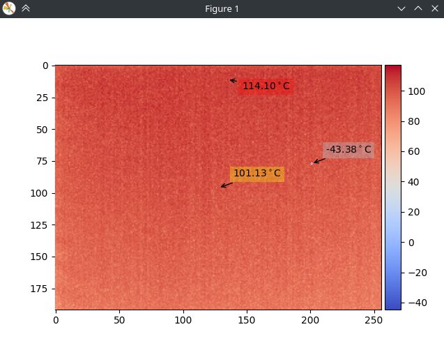
The first thing you'll notice looking at this is that there is a fixed noise pattern imposed on everything. Also, if I point the camera at something hot, it does indeed appear to kinda work. For example, here is my soldering iron:
Since these offsets or non-uniformities appear to be static, I thought of just creating a noise map with offsets for each pixel and subtracting that from the image every time we capture a frame. Thanks FLIR for the tip btw 😉.
In order to practically implement this we first close the shutter. Calculate the average of the entire frame, and then build a noise map based on how far away each pixel is from the average. This way, we get a correction matrix we can apply on every subsequent frame capture to compensate for the offsets. The shutter is a part of the camera that just covers the sensor to make it look at something of uniform temperature. This shutter is here exactly to correct this sort of non-uniformities, also known as flat-field correction, or FFC.
def read(self, raw = False) -> Tuple[bool, np.ndarray]:
    ret, frame_raw = self.cap.read()
    self.frame_raw_u16: np.ndarray = frame_raw.view(np.uint16).ravel()
    frame_visible = self.frame_raw_u16[:self.fourLinePara].copy().reshape(self.height, self.width)
    if raw:
        return ret, frame_visible
    if self.reference_frame is not None:
        frame_float = frame_visible.astype(np.float32)
        corrected_frame = frame_float - self.reference_frame + self.offset_mean
        corrected_frame = np.clip(corrected_frame, 0, 65535)
        frame_visible = corrected_frame.astype(np.uint16)
    return ret, frame_visible


def calibrate_raw(self) -> None:
    self.reference_frame = None
    self.offset_mean = 0.0
    self.dead_pixels_mask = None
    self.cap.set(cv2.CAP_PROP_ZOOM, 0x8000) # close shutter
    sleep(0.3)  # wait for the shutter to close
    self.flush_buffer()
    # by issuing this command faster than once per second, we can keep the shutter closed
    self.cap.set(cv2.CAP_PROP_ZOOM, 0x8000)
    ret, frame_visible = self.read(raw=True)
    if ret:
        self.reference_frame = frame_visible.astype(np.float32)
        self.offset_mean = np.mean(self.reference_frame)
    else:
        raise RuntimeError("Failed to capture reference frame")
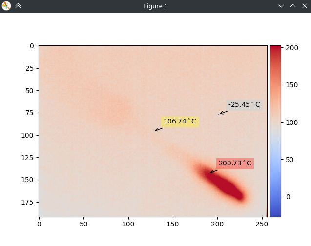
And after the above modifications, we get this:
And as you can see, it works pretty well. However, do you see another issue? On the right, there is a dead pixel reporting some garbage data.
The algorithm to correct for this one took me a bit longer than I expected because I needed to make it work for both temperature ranges. (The T2S+ has two temperature ranges; the standard one is -20°C to 120°C and a high-temperature one for hotter stuff, 120°C-450°C.) The dead pixel finding is done by doing some statistics and finding pixels that deviate a lot from the average value of the sensor with the shutter closed, and then saving those into a so-called dead pixel mask. Then, when capturing a frame, we simply run OpenCV inpainting on only those pixels. This prevents the image from being blurred, and we retain as much detail (and noise) as possible. So, this is what the calibration and sampling routines looked like in the end:
def read(self, raw = False) -> Tuple[bool, np.ndarray]:
    ret, frame_raw = self.cap.read()
    self.frame_raw_u16: np.ndarray = frame_raw.view(np.uint16).ravel()
    frame_visible = self.frame_raw_u16[:self.fourLinePara].copy().reshape(self.height, self.width)
    if raw:
        return ret, frame_visible
    if self.reference_frame is not None:
        frame_float = frame_visible.astype(np.float32)

        corrected_frame = frame_float - self.reference_frame + self.offset_mean

        corrected_frame = np.clip(corrected_frame, 0, 65535)

        if self.dead_pixels_mask is not None:
            inpaint_radius = 3
            corrected_frame = cv2.inpaint(corrected_frame, self.dead_pixels_mask, inpaint_radius, cv2.INPAINT_TELEA)

        frame_visible = corrected_frame.astype(np.uint16)

    return ret, frame_visible

def calibrate_raw(self, quiet=False) -> None:
    '''Camera calibration for cameras that return raw data only'''
    self.reference_frame = None
    self.offset_mean = 0.0
    self.dead_pixels_mask = None
    # uniformity correction
    sleep(0.5)
    self.cap.set(cv2.CAP_PROP_ZOOM, 0x8000) # close shutter
    sleep(0.3)  # wait for the shutter to close
    self.flush_buffer()
    # by issuing this command faster than once per second, we can keep the shutter closed
    self.cap.set(cv2.CAP_PROP_ZOOM, 0x8000)
    ret, frame_visible = self.read(raw=True)

    if ret:
        self.reference_frame = frame_visible.astype(np.float32)
        self.offset_mean = np.mean(self.reference_frame)
    else:
        raise RuntimeError("Failed to capture reference frame")

    # dead pixel correction
    frame_visible_float = frame_visible.astype(np.float32)
    min_val = np.min(frame_visible_float)
    max_val = np.max(frame_visible_float)
    threshold_margin = (max_val - min_val) * 0.05  # Adjust the multiplier as needed
    threshold = min_val + threshold_margin

    self.dead_pixels_mask = cv2.inRange(frame_visible_float, 0, threshold).astype(np.uint8)

    if not quiet:
        print(f"Found {np.count_nonzero(self.dead_pixels_mask)} dead pixels")
        print(f"At: {np.argwhere(self.dead_pixels_mask)}")
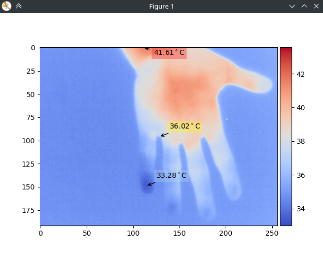
Another aspect that changed for the T2S+ V2 compared to the V1 is the core and shutter temperature. From what I understand, the core temperature should reflect the temperature of the sensor itself (or its substrate to be exact), while the shutter temperature is the temperature of the shutter so that we know what temperature we are looking at with the shutter closed.
I started by dumping the "4 line data". The way these cameras communicate with the computer is through a single USB camera device, where writing to the camera is done by writing to the CAP_PROP_ZOOM register. And reading is done through 4 rows on the bottom of the image. After dumping the data from the special lines, I found that only 3 values actually change:
> diff ./run1.txt ./run2.txt
1,2c1,2
< Off: 0; u16: 6436
< Off: 1; u16: 7847
---
> Off: 0; u16: 6454
> Off: 1; u16: 7881
258c258
< Off: 257; u16: 619
---
> Off: 257; u16: 604
Two of them are related to the statistics of temperature readings of the sensor itself located at the start of the first line (offset 0 and 1). And the other one, located at the start of the second line (offset 257), was likely the core temperature.
Thankfully, with Ghidra and hints from the error report by the thermometry shared object, I was able to get the formula to convert the raw register value to an actual Celsius value.
if (shutTemper < 2049) {
    floatShutTemper = (float)(ulong)(uint)shutTemper;
    fVar15 = 0.625;
}
else {
    floatShutTemper = (float)(0xfff - (uint)shutTemper);
    fVar15 = -0.625;
}
floatShutTemper = (floatShutTemper * fVar15 + 2731.5) / 10.0 + -273.15;
However, when I actually implemented this formula in the Python script, I noticed that the temperature in this register quickly increases after power on and gets quite hot, which suggests it is placed somewhere close to a hot spot of some sort, maybe even on die of some processing IC (more on this in the teardown section). If I use this value in the temperature calculations for the entire image, then it starts to drift very rapidly and shows wrong temperatures. So for now, the value is just a hard-coded value that you'd adjust depending on where you are using the camera.
At this point, the modified hacklib was able to actually work quite well and display a usable image. I put in a quick PR for the hacklib repo here. However, after seeing my PR be ignored for several months, and no other activity happening in that time either I realized that the hacklib repo is likely dead, so I decided to just maintain my own fork for now located here.
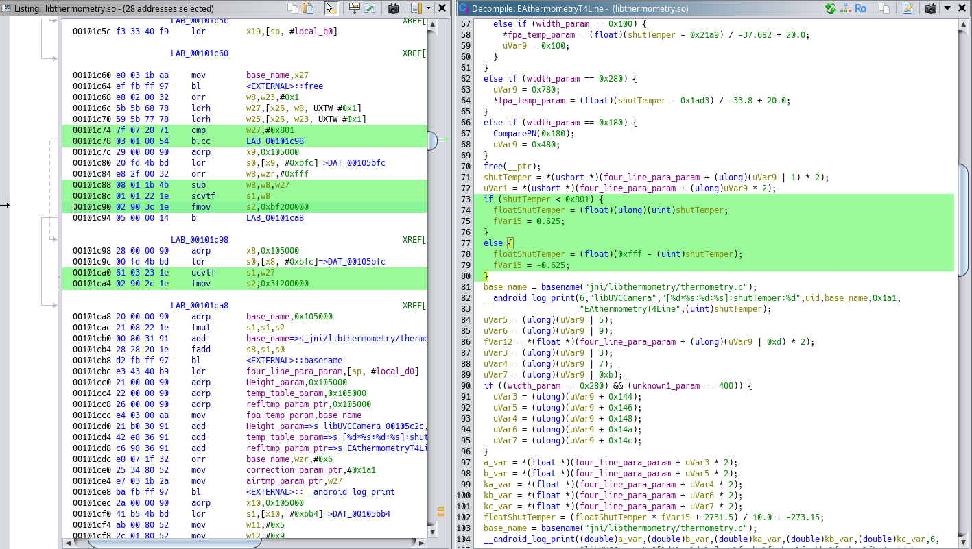
Teardown link
Now, let's get to the fun part. I actually took apart my camera and documented what's inside one of these T2S+ cameras. From what I can tell, I am the first one to do this with one of these specific cameras. There are plenty of teardowns of the FLIR and the P2 Pro cameras, but not the T2S+.
⚠️ You are responsible for any damage that may occur by following this procedure. The author is not responsible for any damages if the user chooses to follow the teardown directions. ⚠️
Let's start with the opening procedure. The camera body consists of two halves: one plastic and one metal. The plastic part is a shell that only has the USB connector attached. The rest is sitting on the metal part. (I learned this even before the teardown by taking a flashlight and shining light through the slightly translucent case). In order to remove the case, you need to undo at least two clips on two neighboring edges. They are located in the middle of the edge, and you can see them by slightly prying up the case first. After you see them, simply press them in gently and apply some force to split the halves apart. Repeat this on the other edges until it opens. Initially, the clips have a tiny bit of weak glue, but thankfully, it's quite brittle and breaks off with ease.
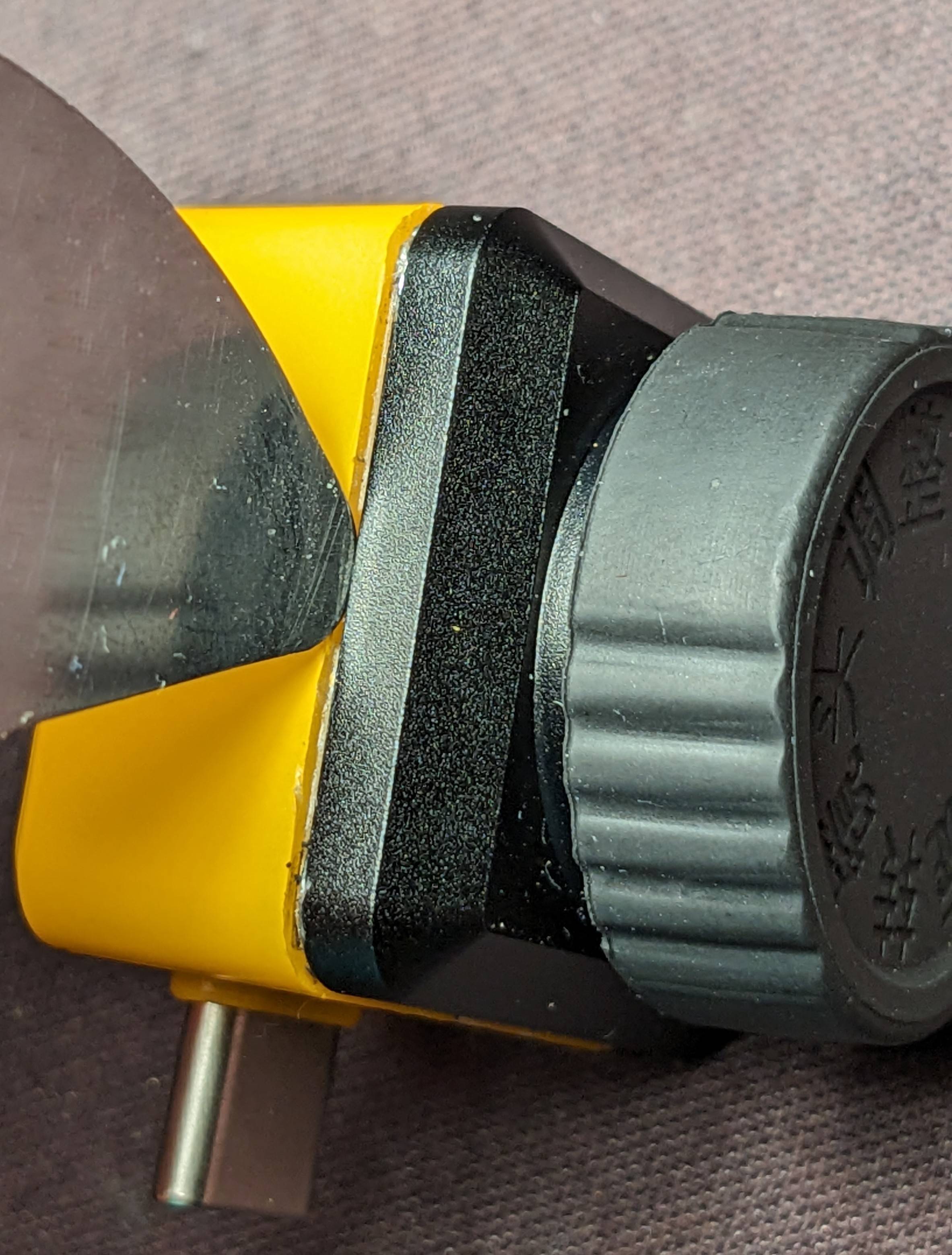
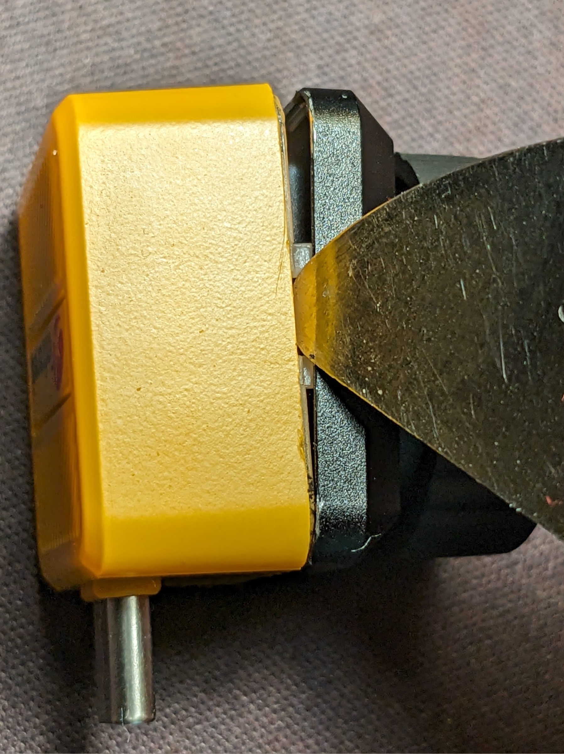
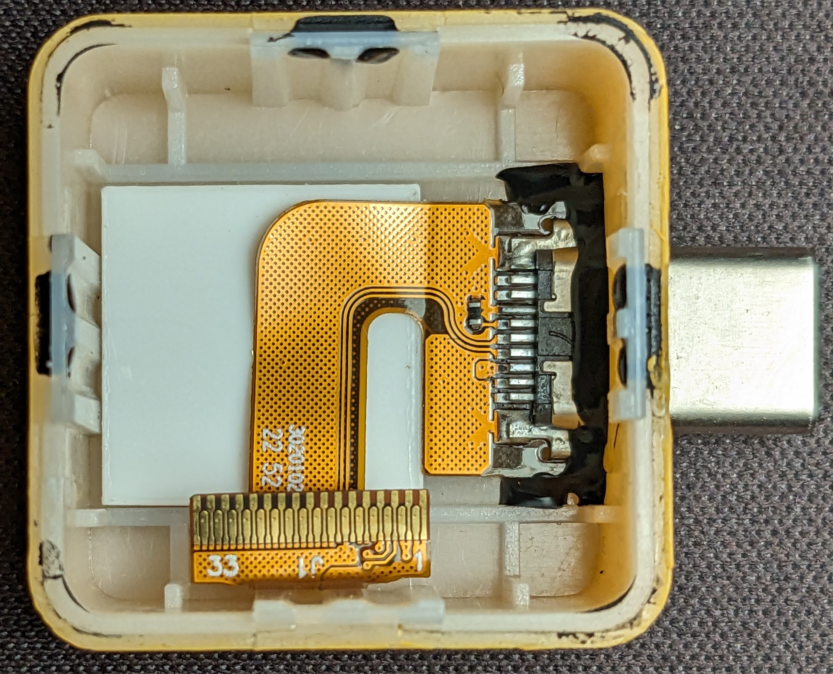
After cracking it open and carefully removing the shell, we are greeted with the board stack attached to the metal body, along with the USB connector connected by a short flat flex and secured with some tape.
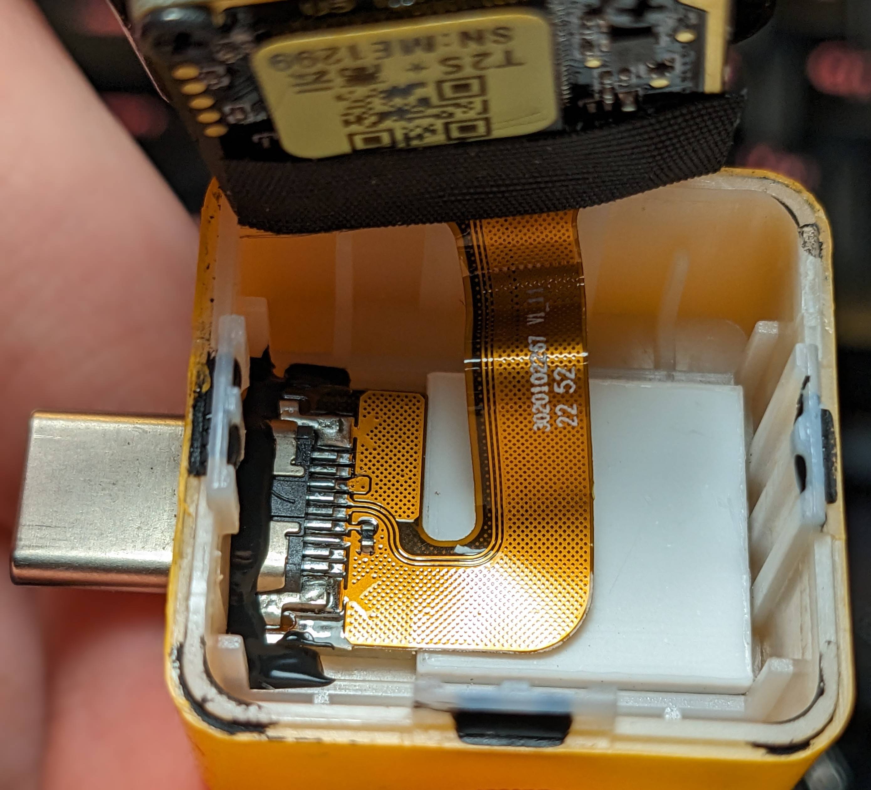
After disconnecting the ZIF connector, we can take a closer look at the bottom case. Here we have the drops of glue on the latches securing the case, as well as the USB port glued in with the same material. The USB port connects with a fairly wide flat flex connector, clearly designed to carry more signals than just the two D+ and D- signals seen here. Additionally, there is a block of plastic that seems to be there just to fill space. There is quite a bit of room for some compact modifications if someone wants to add something in here, such as a better temperature sensor.
Moving to the electronics and optics assembly, we are greeted with a PCB sandwich consisting of two boards.
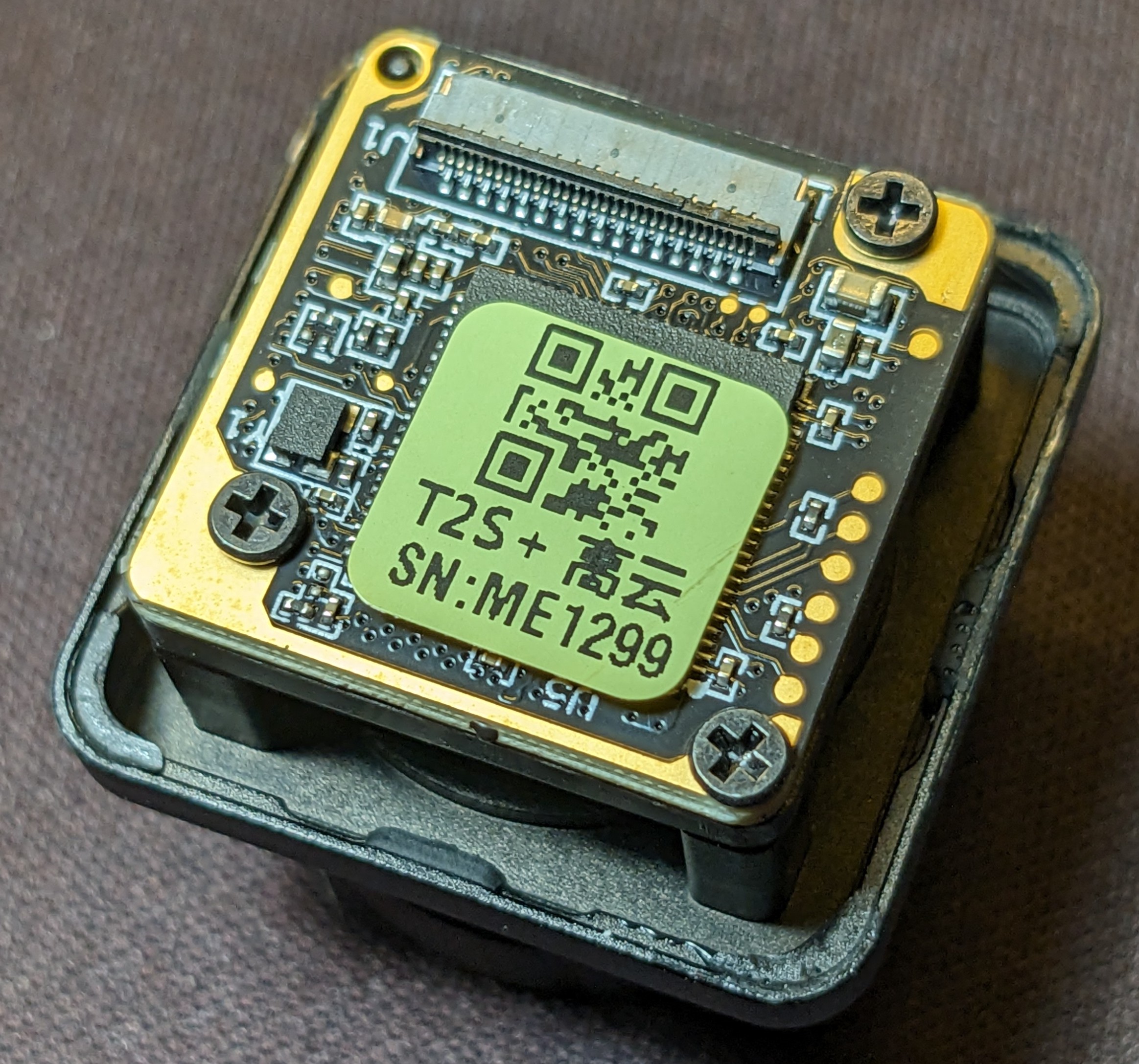
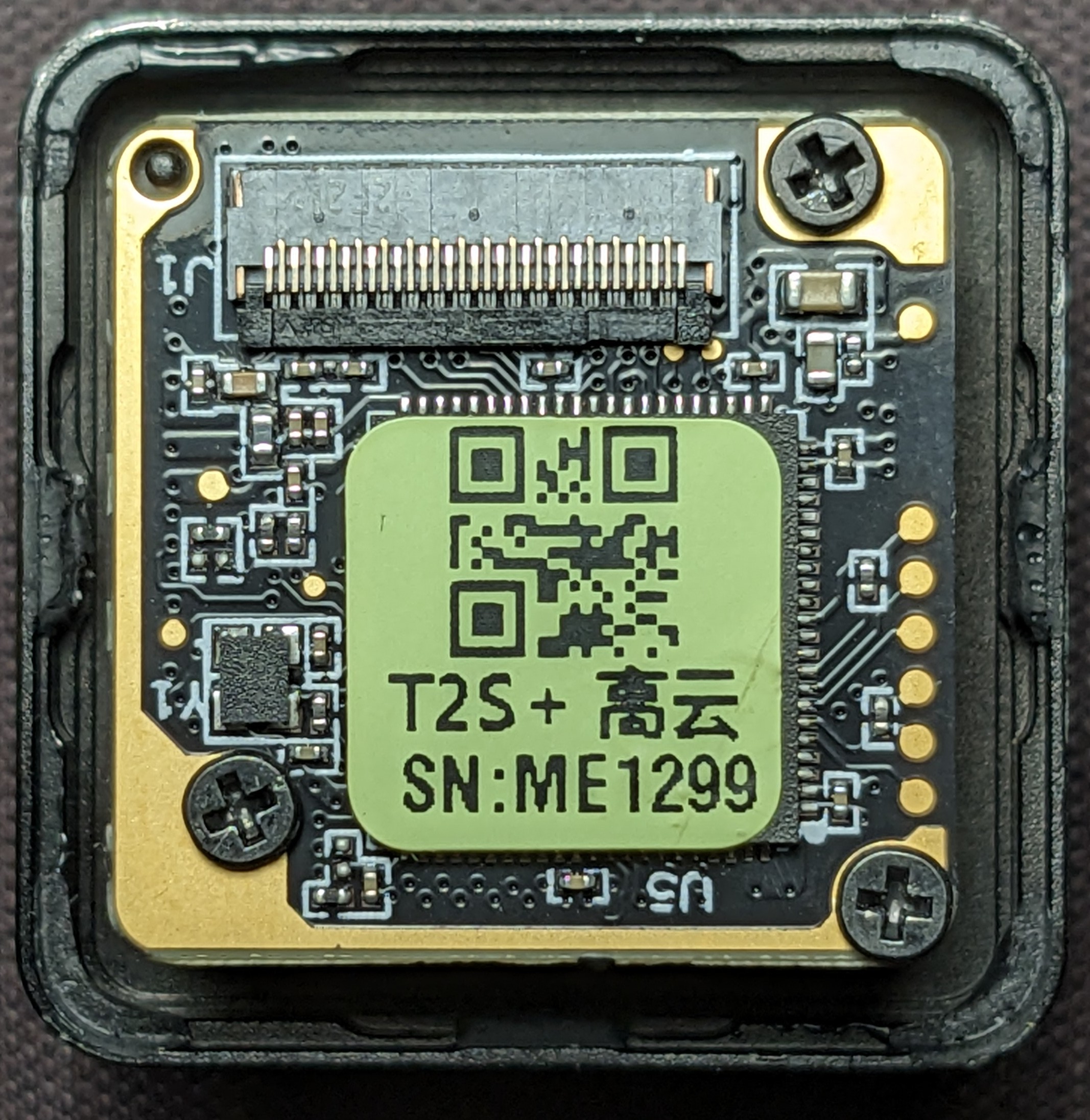
The board attached to the USB connector will be referred to as the top board, while the one with the image sensor will be called the bottom board. So, right after removing the assembly from the plastic case, you will see the top board with a sticker covering some sort of IC marked U5. Right next to the IC, we can see a crystal/oscillator marked Y1 and the connector used for the USB cable marked J1. Other than that, there is a handful of passive components consisting of MLCCs and a few resistors. Interestingly, the board also contains quite a few test points. The most intriguing one is the six-point test pad on the edge of the board; could that be a debugging interface like JTAG?
Let's remove the sticker and see what's hiding underneath...
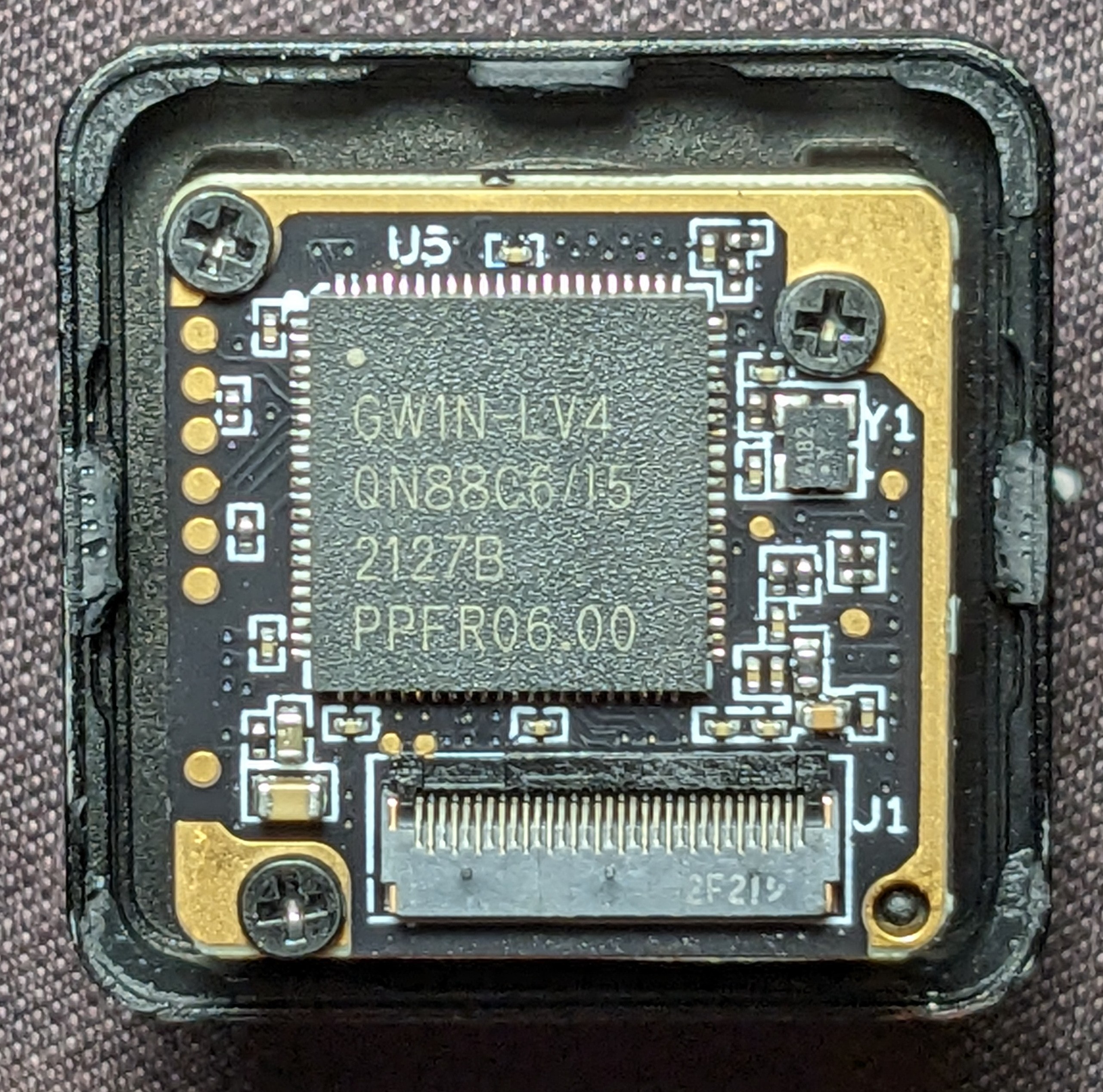
And it's a GOWIN FPGA! A GW1N-LV4QN88C6I5, to be exact. So, the forum rumors about the FPGA being
removed and
replaced with an ASIC appear to be false. However, let's take a look at the rest of the board to get a general idea
of what is happening before we start diving into the specifications of the chip.
In order to progress through the PCB sandwich, we need to remove the three screws holding the assembly together. At this point, we need to be more careful since there is nothing keeping the board with the sensor in place. Since the sensor is just a bare die glued to the PCB, it's a bit fragile. So, with care, trying to keep the bottom board in position, we slowly work the top board out of its mezzanine connector holding it in place.
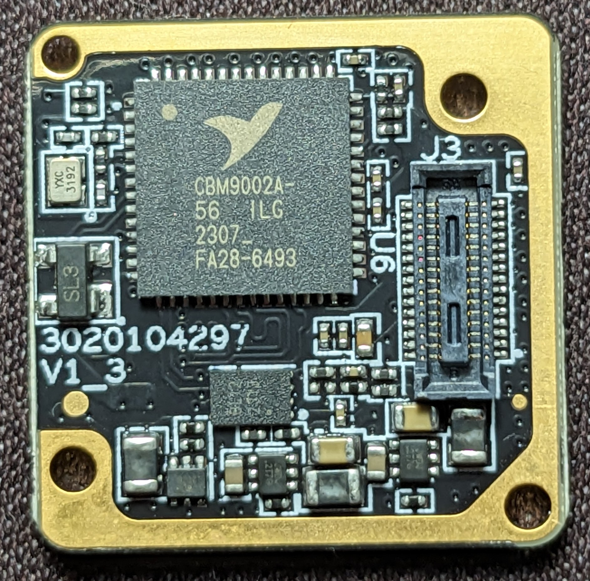
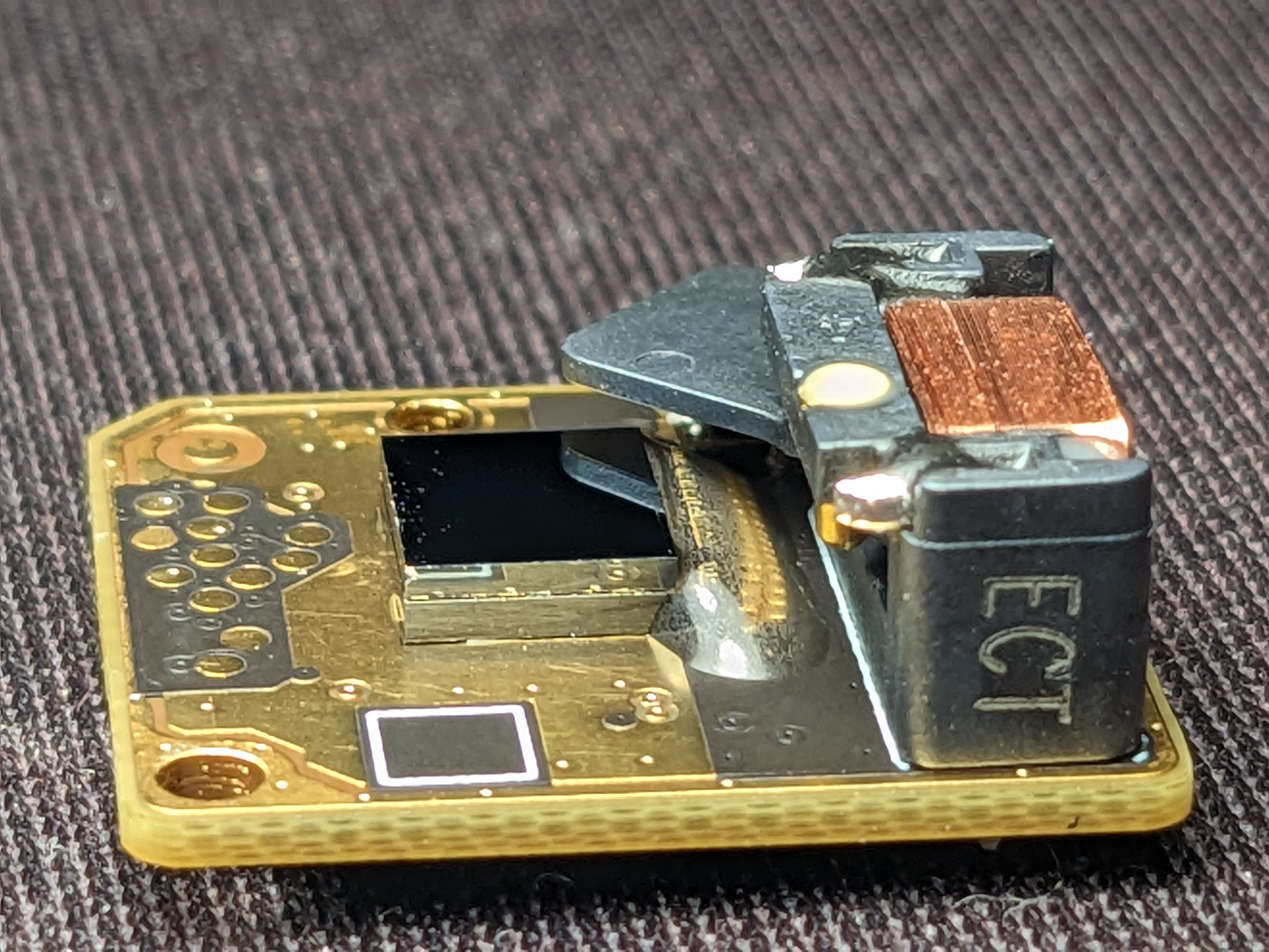
On this side, we are greeted with a bit more interesting stuff. The largest component (U6) is a
CBM9002A-56, which appears to be a Cypress FX2LP clone, likely of a CY7C68013A or one of
its variants. These are "single-chip integrated USB 2.0 transceiver" ICs. This chip handles the USB
communication with the host machine and is likely being fed by the parallel inputs that this series supports.
This explains why the camera shows up as a Cypress Semiconductor device in lsusb.
Next to this chip is the required 24 MHz crystal oscillator, with ESD protection for the USB lines marked
SL3 right next to the crystal. A tiny EEPROM is located below the USB interface chip,
marked BL12 2313. The board interconnect is labeled J3. Finally, there are three DC-DC
converters marked with JWDJ 2T7G. The EEPROM is likely connected to the FPGA since I don't think the
USB IC supports EEPROMs.
Next, we can move over to the bottom PCB, the one that contains the image sensor on the other side. However, we have a pesky QR code blocking our view.
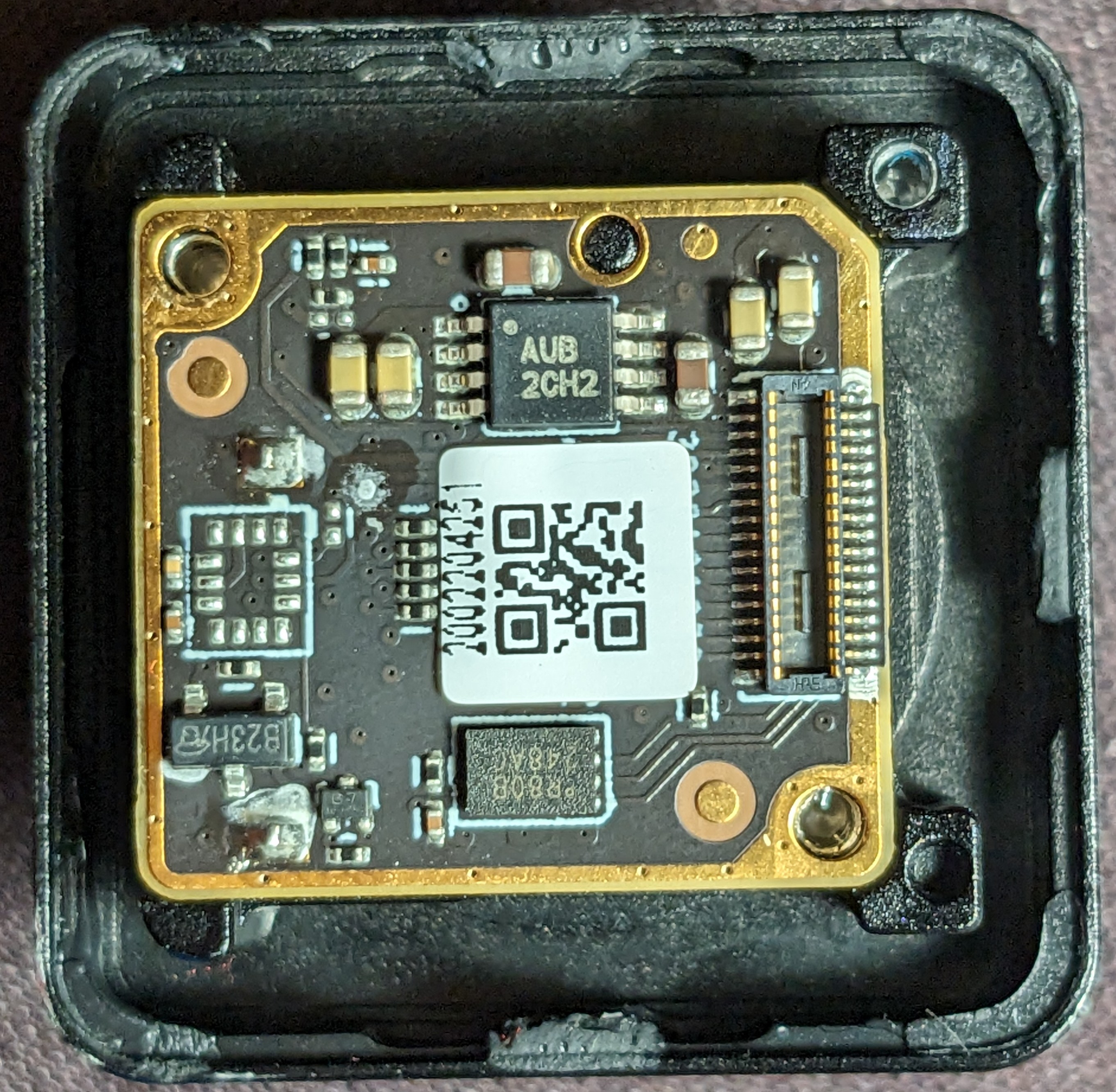
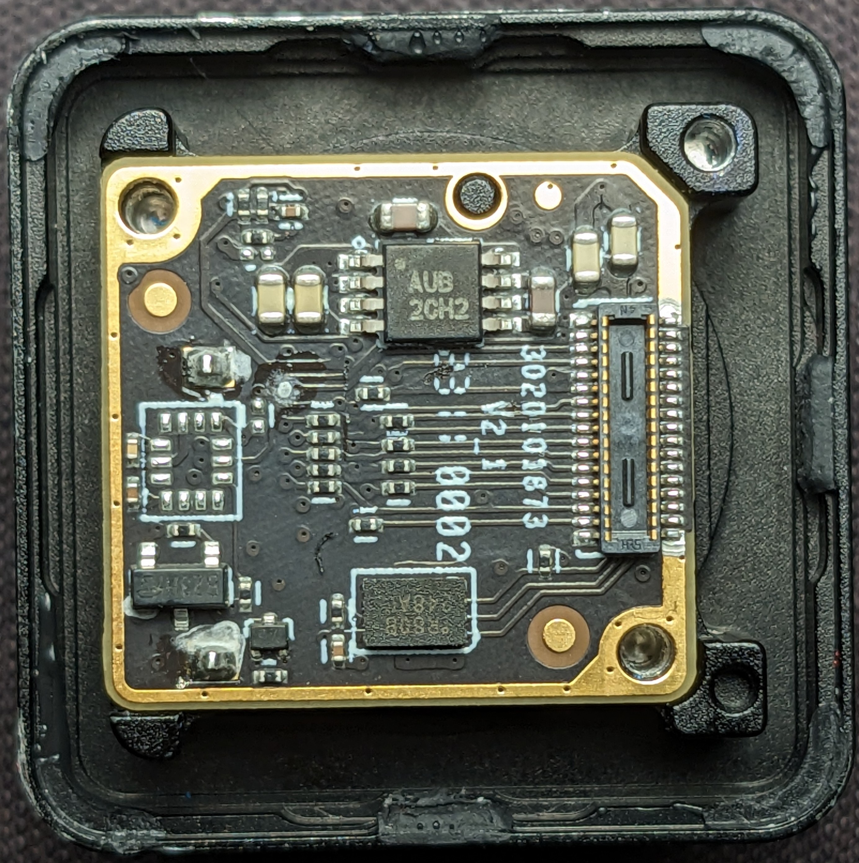
After removing it, we see that it was covering what looks like termination resistors — 11 termination resistors, to
be exact. This suggests that the readout is happening through some sort of 8-bit parallel bus, possibly Octal SPI.
On one side of the board, there is something resembling an LDO marked AUB 2CH2, judging by the amount
of decoupling around it. On the opposite side, there is another EEPROM IC, this time with the markings
R80B 248AC.
Since this sits on the image sensor-containing board itself, I would guess it contains some calibration, serial
number, or type information for the top board to identify what it's communicating with. Right next to it is a tiny
three-pin part simply marked 67, with a resistor next to it. This could potentially be a OneWire
temperature sensor, but I don't have any way of confirming that. Finally, there is what appears to be an N-channel
MOSFET for closing the shutter, as well as a mysteriously unpopulated spot next to it.
Now, let's flip the board over and take a look at the image sensor itself. It appears a bit underwhelming, resembling just an empty piece of silicon.
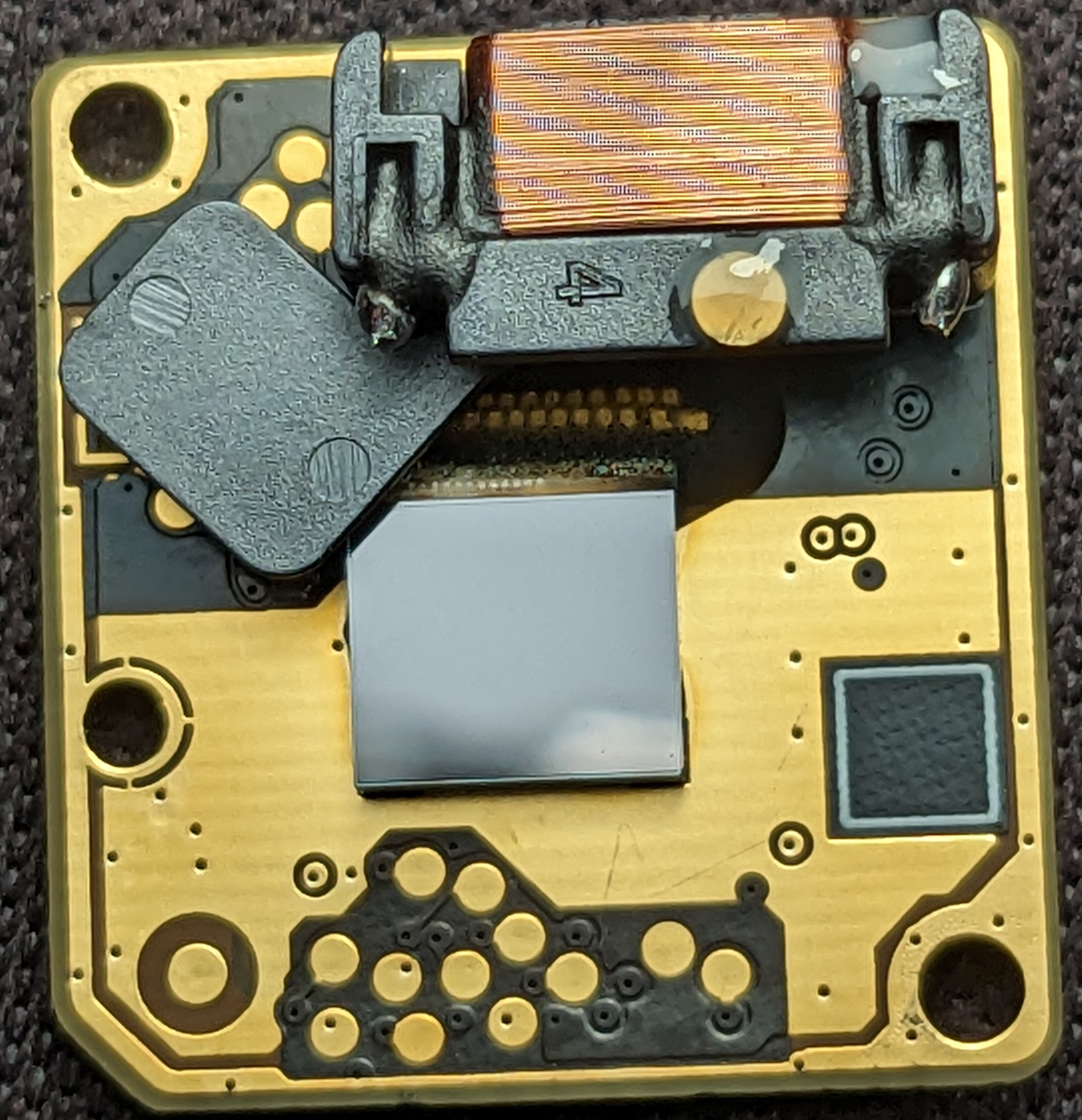
And that's because it is. If we tilt the board to the side, we can see that there are two pieces of silicon. The lower one is where the actual image sensor and readout electronics are located; this is confirmed by bond wires covered in epoxy coming off from one side. The upper piece of silicon is just a cap made of silicon that has been bonded on top of the sensor to protect the fragile microbolometers in the image sensor.
Other than the sensor itself, we can see the shutter, which is just a piece of plastic with a solenoid. I don't think this camera can measure the shutter temperature at all, as indicated by the lack of any thermometers in the area.
Also, we see 12 test points, which sounds suspiciously similar to the 11 resistors we found on the back. I don't have the means to probe them right now, but I would expect that someone with a bit more dedication and willpower would definitely be able to read this out.
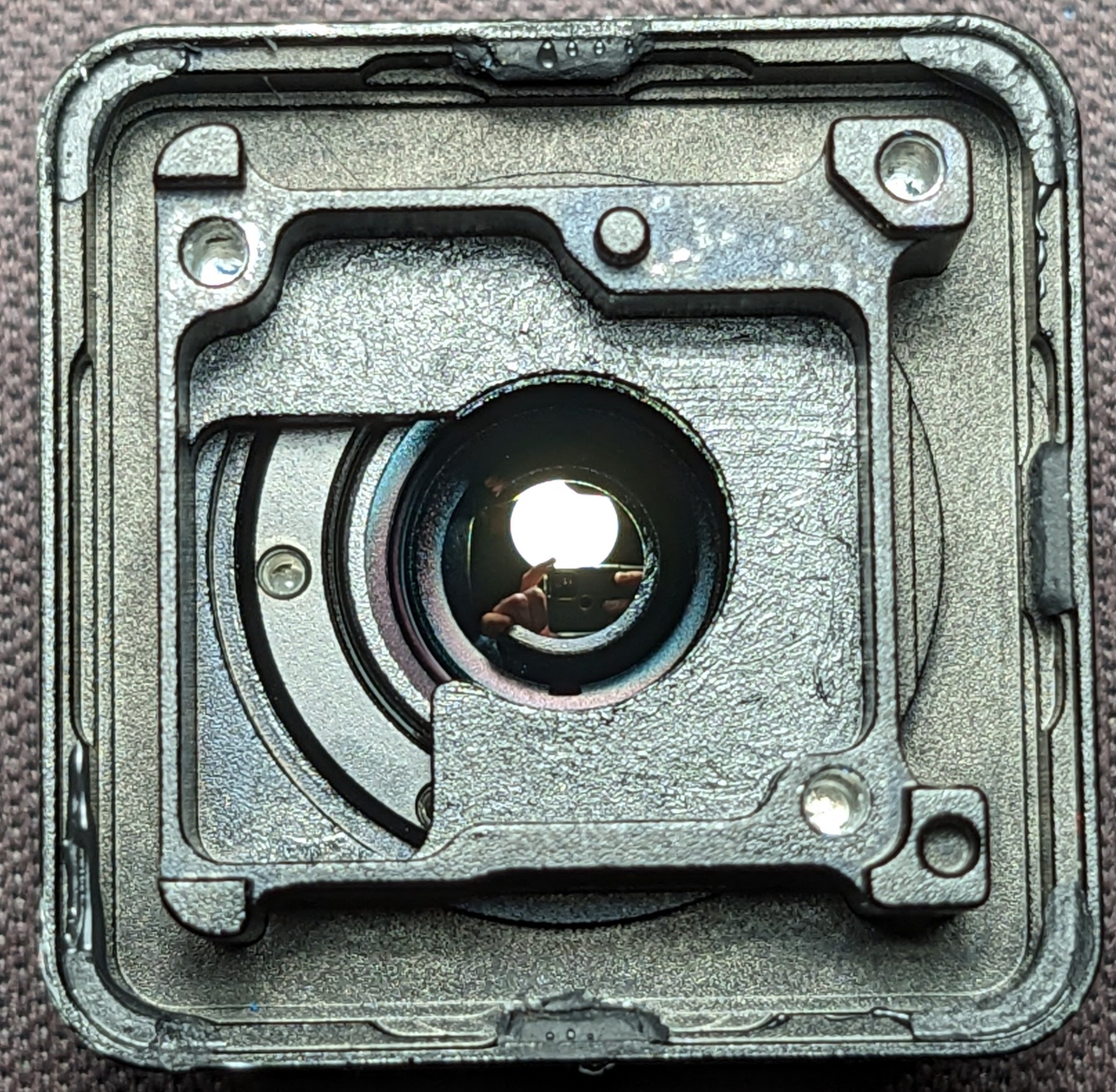
Regarding the lens assembly, it is built quite well, made out of metal. The focus ring is smooth and has a very wide range of focal distances, ranging from infinity to just a few millimeters away from the lens.
At this point, I am a bit too busy to dive deeper into reverse-engineering the hardware. I hope this will be useful for someone looking to start hacking on that front as well. It should be possible to read it out even with something like a mid-range MCU and display the output on one of the cheap AliExpress IPS displays, making for a great standalone camera with zero boot time and a reasonable price.
Lock-in Thermography link
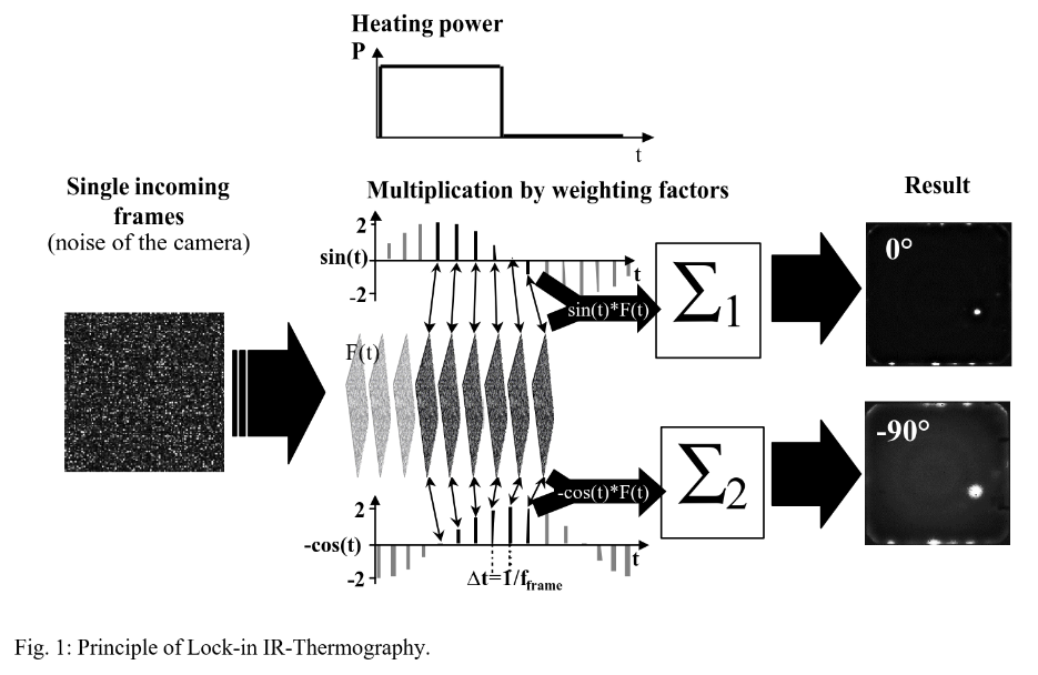
While finishing this write-up, I stumbled upon a post by outside five sigma that talked about Lock-in IR Thermography. After reading the paper mentioned in the post, the concept seemed simple: modulate the power supply of a circuit and capture it with an IR camera while doing so. Then, multiply each frame by a sine and cosine scaled factor in phase with the modulation. Finally, average these frames over some integration time. This creates in-phase and quadrature thermal images of the device under test, amplifying the hotspots and improving the thermal resolution of the image. Figure 1 from the paper shows the concept quite well:
After seeing how simple the concept is, I was surprised to learn that no one has implemented something similar for these cameras. After a few hours, I already had images, and after some more time wrangling with Matplotlib, I got a nice UI to go along with the proof-of-concept implementation. To demonstrate this technique, I decapped an AD9042 ADC that I had in a ceramic DIP package. A Raspberry Pi Pico and a MOSFET were used to modulate the power to the chip, with the control software issuing ON/OFF commands over serial. This produced very nice results, even with a very low integration time.
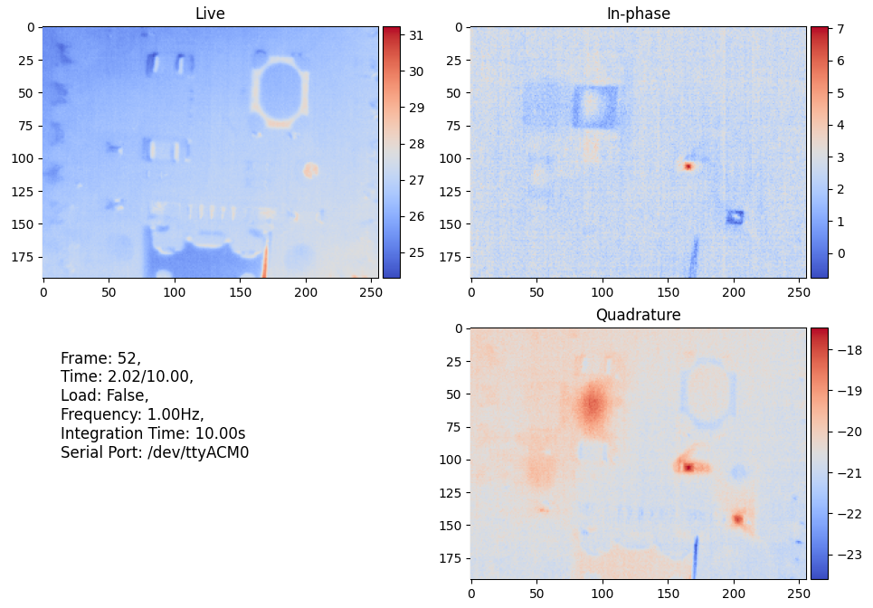
It's not only useful for silicon die debugging; it can also highlight even minute heat sources on PCBs and anything else that can be modulated, including people. In the image below, the camera was pointed at a Raspberry Pi Pico that was programmed to blink the LED at a rate of 10 Hz. After only 10 seconds of integration, we can already see the heat from the LED, its resistor, and the DC-DC converter, even though none of these are visible in the live feed (the small dot you see is the fiducial reflecting other heat sources in the room).
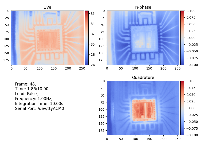
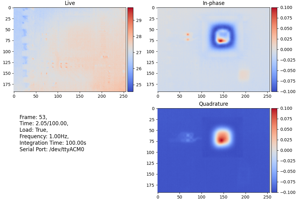
After pointing the camera at the RP2040 itself and integrating for a little over a minute (100 seconds), we are able to clearly see the heat inside the QFN package, a bit of heat from the QSPI flash, and most interestingly, from the VBUS detect voltage divider and its copper traces. This is significant because that voltage divider only dissipates about 1.6 mW of power, which highlights the impressive sensitivity of this imaging method.
The code for this was literally the formula described in the paper. If you wish to see the source code or simply use it, everything can be found in the same repo. PRs are welcome!
Maybe at some point, I will come back to this and try to reverse-engineer the sensor itself and the "4 line data" to get the temperature offsets for the T2S+ v2 automatically, but for now, I will declare the thermal camera project complete.
Accompanying YouTube video:
